Research
Summary
We have broad research interests and extensive experiences in material growth, optical and electrical characterizations, device physics and fabrication, and optical communications and interconnects. Quantum geometry and band topology of emerging materials and Computational spectroscopy and intelligent sensing are two typical research topics within the group.
Quantum geometry and band topology of emerging materials
Geometry is a vibrant contemporary math branch originated in ancient Greece. The research on geometry has significant impacts on various disciplines such as art, music, physics, and engineering. In physics, geometry plays a critical role in describing both macroscopic and microscopic physical phenomena. For example, the essence of Einstein’s theory of general relativity lies in the geometry of spacetime. In microscopic world, the quantum geometry of electron wavefunctions, i.e., Berry curvature and quantum metric, largely affect their properties in both ground and excited states.
Global quantum geometric properties can determine band topology, which is often characterized by a quantized integral of local quantum geometric term(s) over a closed manifold, e.g., Bouillon zone. The materials with nontrivial topological properties have attracted significant attentions recently. For example, graphene is arguably the simplest topological material with nontrivial winding numbers around its bulk Dirac points. The celebrated topological insulators have nontrivial Z2 nvariants as manifested by their boundary Dirac cones.
Interestingly, even local quantum geometry can be critical for light-matter interactions, especially in nonlinear regime. Recently, we revealed the rich, tunable and reconfigurable quantum geometric properties in a dual-gate twisted double bilayer graphene (TDBG) device through the nonlinear linear and circular bulk photovoltaic effects (BPVE) as illustrated in the Figure 1 below.
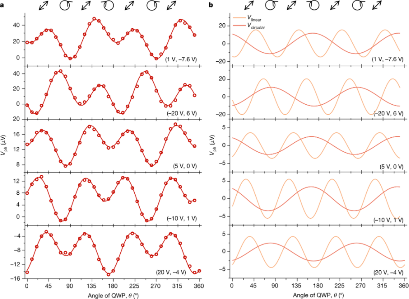
Figure 1. Reconfigurable nonlinear photoresponse in a dual-gate TDBG device. a, Nonlinear photovoltage (Vph) as a function of the angle of the quarter-wave plate (QWP) (q) at different gate voltage biases (VBG, VTG), measured at T = 79 K and λ = 5 μm. The incident light first passes through a half-wave plate (direction of fast axis fixed) and then a quarter-wave plate (direction of fast axis changing on rotation). The polarization states of the incident light are denoted at the top of the figure. The offset of the linear polarization state from q = 0 is caused by the half-wave plate, of which the fast axis is approximately 60° away from the z axis in laboratory coordinates. Two components, Vlinearand Vcircular, with the periodicity of 90° and 180° can be identified by fittings. b, Constructed Vlinear and Vcircular from fittings, from which a doubled periodicity of Vcircular compared to Vlinear is observed. The amplitudes and phases of both components are tunable by gate voltage biases (VBG, VTG). Adapted from Nature 604, 266-272 (2022).
The results in Figure 1 are significant for a few reasons. First, it may be possible to extract the quantum geometric properties of TDBG from the nonlinear photoresponses which depend on the excitation light polarization and wavelength. Second, both linear and circular nonlinear signals have been observed, implying the strong symmetry breaking in this twisted system. Third, the photoresponse is reconfigurable by the gate biases. Such reconfigurability is critical for building intelligent sensors, as will be discussed below.
Currently, our group is further investigating the nonlinear properties of other emerging quantum materials, focusing on the roles of quantum geometry and band topology.
Computational spectroscopy and intelligent sensing
Investigating how materials, devices and systems respond to EM waves with different frequencies and physical properties is the cornerstone of electrical engineering. In fact, EM wave (or light) consists of very rich information including spectrum, power, polarization, coherence, and angular momentum. Traditionally, detection of different physical properties of light requires different instruments. For example, power meter, spectrometer and polarimeter are utilized for the detection of light intensity, spectrum, and polarization state, respectively. Many of these instruments can be very bulky and sometimes they occupy a large space on an optical table.
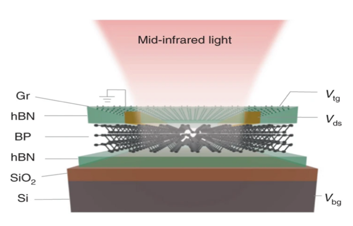
Figure 2. Schematic of the BP spectrometer. It consists of a hBN/BP/hBN heterostructure capped by monolayer of graphene on a silicon dioxide-covered silicon substrate. Graphene and the silicon substrate are used as the top and back gates, respectively. The source–drain electrodes are composed of chromium/gold. Gr, graphene. Adapted from Nature Photonics 15, 601-607 (2021).
Here we use our recently demonstrated single element black phosphorus spectrometer to illustrate our proposed concept of computational spectroscopy. The device schematic is shown in Figure 2. In this device, the bandgap of black phosphorus can be tuned by the electric field, leading to reconfigurable spectral responses in the infrared wavelength range.
The operation procedures of our single-element black phosphorus are illustrated in Figure 3 and its caption. In short, the spectroscopy function, which usually can only be accomplished by a rather complex instrument (or at least an array of devices), can now be realized using a single on-chip device at microscale and a well-designed, explicit algorithm.
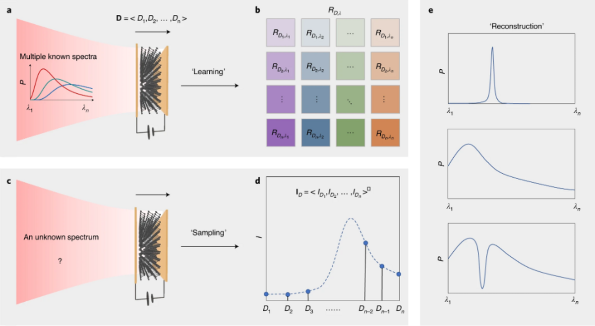
Figure 3. The operational principle of the single-detector BP spectrometer consists of three steps: learning, sampling, and reconstruction. a, Schematic of the learning process. The photoresponse of BP (the dark grey layered material) can be tuned by the electric displacement (D) between two parallel metallic plates. b, The responsivity matrix RD,λ of the BP spectrometer, which depends on the biasing displacement field (D) and the incident light wavelength (λ), is ‘learned’ from the photoresponses to a group of known spectra (illustrated by the red, green, and blue curves in a under different biasing displacement fields). c, Schematic of the sampling process. For the incident light with an unknown spectrum, the photocurrent in the BP detector is sampled as a function of the electric displacement D. d, The sampling process generates the photocurrent vector ID. e, Schematics of three reconstructed spectra. From top to bottom, the spectra represent a narrowband emission, a broadband emission, and an absorption feature of certain gas molecules. Reconstruction of the unknown spectra leverages the RD,λ and ID as discussed in a–d. Adapted from Nature Photonics 15, 601-607 (2021).
Inspired by the operational principle of single-element black phosphorus spectrometer, we have also established a general “intelligent sensing” concept, leveraging the tunable quantum geometric properties of TDBG as discussed above. The operational principle is illustrated in Figure 4. In this sensor, we first measure the nonlinear photoresponses of the TDBG device as the function of top and bottom gate biases, thus generating a photoresponse image (as shown in the left of Figure 4). For light with different wavelength, power, and polarization state, obviously the photoresponse image will be distinct. As a result, it should be possible to sense various physical properties of the unknown light by measuring its photoresponse image. However, in practice, it is not feasible to model the complex TDBG device accurately and interpret the photoresponse image based on explicit algorithms. We proposed to use the convolutional neural network (CNN) to decipher the photoresponse image. Previously CNN has been widely used for image recognition and classification. Here, we first use the photoresponse images generated under light with known physical properties to train the CNN, then CNN is used to interpret the photoresponse image under the excitation of unknown light. Such a scheme is very successful and challenges our conventional wisdom of sensing. Previously, detection of different physical properties of light (power, spectrum, polarization etc.) requires different instruments. Here we leverage a photoresponse image to capture the entire information of light and then a trained CNN successfully deciphers the information, as illustrated in Figure 4.
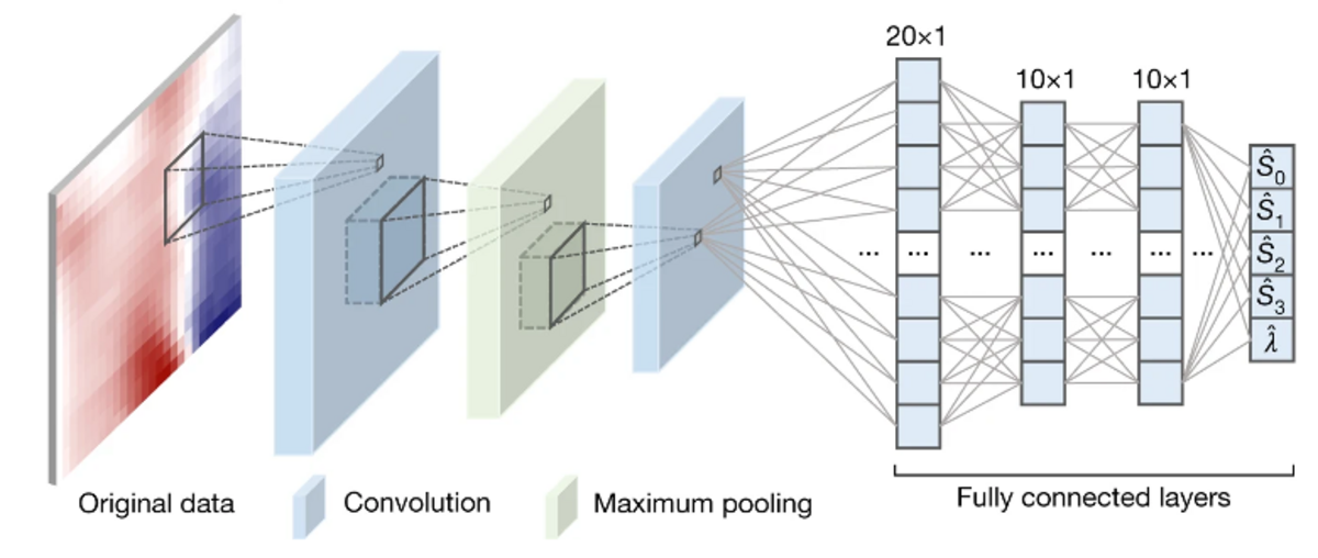
Figure 4. Schematic of the convolutional neural network (CNN) used for the demonstration of the polarimeter and wavelength detection. The input layer is the measured 20×26-pixel photovoltage mapping, and the output is a five-element vector, ( Ŝ0, Ŝ1, Ŝ2, Ŝ3, λ̂). The hidden layers consist of the first convolution layer, the maximum-pooling layer, the second convolution layer and three subsequent fully connected layers. Stokes parameters can be directly calculated based on ( Ŝ0, Ŝ1, Ŝ2, Ŝ3). The wavelength labels λ̂=∓1 correspond to 5 µm and 7.7 µm, respectively. Adapted from Nature 604, 266-272 (2022).
As discussed in the “News and view” by Song and Chong, further developments of this concept may lead to disruptive sensing technologies, which are not limited to sensing of EM waves.
Collaborations
Our group collaborates closely with Prof. Fan Zhang of University of Texas at Dallas, Prof. Doron Naveh of Bar-Ilan University in Israel, and Prof. Ashwin Ramasubramaniam of University of Massachusetts Amherst.
Further reading
C. Ma, S. Yuan, P. Cheung, K. Watanabe, T. Taniguchi, F. Zhang, and F. Xia, “Intelligent infrared sensing enabled by tunable moiré quantum geometry,” Nature 604, 266-272 (2022).
C. Chen, C. Li, S. Min, Q. Guo, Z. Xia, D. Liu, Z. Ma, and F. Xia, “Ultrafast silicon nanomembrane microbolometer for long wavelength infrared light detection,” Nano Letters 21, 8385-8392 (2021).
S. Yuan, D. Naveh, K. Watanabe, T. Taniguchi, and F. Xia, “A wavelength-scale black phosphorus spectrometer,” Nature Photonics 15, 601-607 (2021).
B. Deng, C. Ma, Q. Wang, S. Yuan, K. Watanabe, T. Taniguchi, F. Zhang, and F. Xia, “Strong mid-infrared photoresponse in small-twist-angle bilayer graphene,” Nature Photonics 14, 549–553 (2020).
C. Ma, Q. Wang, S. Mills, X. Chen, B. Deng, S. Yuan, C. Li, K. Watanabe, T. Taniguchi, X. Du, F. Zhang, and F. Xia, “Moiré band topology in twisted bilayer graphene,” Nano Letters 20, 6076-6083 (2020).